
The Engineer Who Owns the Channel: Signal and Power Integrity as a Career
Almost nobody sets out to be a signal integrity engineer. The discipline recruits you, usually on the night a board that simulated clean starts failing at temperature. It has also quietly become one of the least substitutable seats in hardware.
Almost nobody plans this career. The discipline recruits you, usually on the night a board that simulated clean starts throwing errors at temperature and you are the one who stays to find out why. It happens again on a different program, and at some point people stop asking you to review layouts as a favor and start writing your name into the plan.
It is worth knowing what that path looks like now, because the work has moved a long way from where most job descriptions still put it.
Why the Market Came Looking for You
Three specifications reset the difficulty in about eighteen months. PCI-SIG released PCIe 7.0 at 128 GT/s in June 2025. JEDEC published HBM4 with a 2048-bit interface at up to 8 Gb/s per pin and up to 2 TB/s per stack. UCIe 3.0 took die-to-die links to 48 and 64 GT/s and stretched sideband reach to 100 mm.
The SI engineers we place describe the change as margin. Same physics, less room, and the interesting failures now sitting in places that used to belong to somebody else.
The Three Rungs, and Which One Pays
Board SI is where you probably started: stackup, impedance control, crosstalk, insertion loss, eye diagrams on the SerDes lanes, in HyperLynx, Sigrity, SIwave or ADS. Real work, and also the most crowded rung.
Power integrity is the second, and the engineers we place call it the rung most people underinvest in. You will know if you did. PDN impedance across frequency, decoupling strategy, regulator stability, and the nerve to tell a design team that their placement is why the rail sags under a workload nobody simulated. Teams that have been burned once tend to hire PI before they hire anything else.
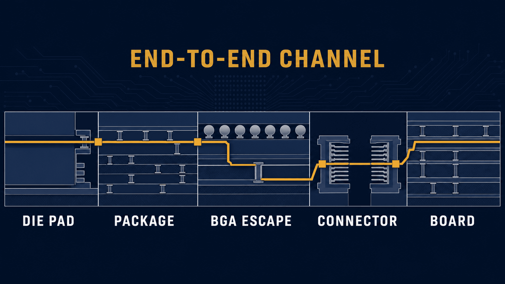
The third rung has no settled title yet. Channel owner, systems SI architect, or just the person who owns the path end to end: die pad, package substrate, interposer, connector, board, and back. The engineers doing it describe closing HBM4's 2048 signals and a UCIe die-to-die budget as one continuous problem. The hiring managers we talk to call it the hardest requisition they write, and from the hiring seat the pool that has closed a channel across all those boundaries is small and mostly employed.
Your Tier Matters More Than Your Years
Years in the discipline count for less here than the class of board and package you have survived.
A 4 to 8 layer design with USB and I2C is a different profession from a 20 layer board carrying DDR5 and PCIe Gen5. Move up again to a 30 to 40 layer datacenter switch board on Megtron 6 or 7, with 112G PAM4 channels and 0.4 mm pitch BGA fanout, and the number of engineers who have shipped one gets very small.
A screening conversation reaches your tier inside five minutes, so make it easy on whoever is reading. Put the layer count and the material near the top, by name, because Megtron 6 is a different sentence from FR-4. Put the data rate and interface beside it, with what you owned on each. And if you have done any package-level SI/PI work in HFSS or SIwave on a substrate or interposer rather than only on a board, lead with that, because it is the half of this discipline where teams are shortest right now.
What Separates Senior From Principal Here
Simulation is table stakes, and the SI engineers we work with are consistent about the line: whether you can correlate a model to a measurement and explain the gap.
That means VNA and TDR work, fixture design, and de-embedding you can defend. IEEE 370-2020 is the standard for electrical characterization of printed circuit board and related interconnects up to 50 GHz, and the engineers we talk to treat fluency in it as a principal-level marker, because two people can measure the same channel and disagree about what they saw.
Glass weave skew, copper roughness, real laminate Dk against datasheet Dk, and what the fabricator actually built rather than what the stackup drawing said. The PCB and SI engineers we place raise these constantly, because that is where the margin quietly went.
What Contract Work Does for This Career
SI and PI work has natural boundaries: a channel design, a correlation campaign, a bring-up debug, a connector or retimer change. Programs need deep expertise for a defined stretch, then need it again at the next platform. That is a career advantage, not a compromise.
It also builds the one asset that matters here. Every engagement adds a class of board, a package technology, a measurement setup and a failure you personally chased. Engineers who move across programs stack up tiers faster than engineers who stay on one product line, which is a large part of why the market pays for them.
From our side of the table, two in three of the engineers we put in front of a hiring manager come out with an offer, which is what happens when the match is made on tier and technology instead of on a title. Our median from submission to placement is about 26 days, so a search started while your current engagement is still running rarely leaves a real gap.
Signal and power integrity has moved from a review squeezed in before release to a seat programs plan around. Prove a channel with a measurement and you are among the least substitutable people in the room, which makes this a good moment to act like it.
Worth a look at the channel-side roles we are hiring for to see what is actually out there, and if there's nothing publicly posted, we'll reach out to you.
FAQ
Frequently Asked Questions
What Does a Signal Integrity Engineer Actually Do?
On the board side: stackup and impedance control, crosstalk and insertion loss budgets, and eye diagrams on the high-speed lanes, simulated in HyperLynx, Sigrity, SIwave or ADS and then measured with a VNA or TDR. At package level the same discipline covers the substrate and interposer. The job is owning whether a signal arrives intact across every boundary it crosses, and being able to prove it rather than assert it.
What Is the Difference Between Signal Integrity and Power Integrity Work?
Signal integrity is about the data path: reflections, crosstalk, loss and jitter on a channel. Power integrity is about delivery: PDN impedance across frequency, decoupling strategy and regulator stability under real workloads. They use overlapping tools and get combined into one job title constantly. The engineers we place say power integrity is the half most people underinvest in, and the half teams hire first once they have been burned.
What Separates a Senior SI Engineer From a Principal One?
Measurement, according to the SI engineers we work with. Simulation is table stakes at senior level. The principal-level signal is correlating a model to a measurement and explaining the gap: fixture design, de-embedding you can defend under IEEE 370-2020, and an account of where glass weave skew, copper roughness or real laminate Dk took the margin that the datasheet said you had.
Is Signal Integrity a Good Discipline for Contract Work?
It suits it unusually well, because the work has natural boundaries: a channel design, a correlation campaign, a bring-up debug, a connector or retimer change. Programs need the depth for a defined stretch and then need it again at the next platform. Moving across programs also stacks up board and package classes faster than staying on one product line, and tier is what this market actually pays for.

Written by
Jason Eisenberg
Head of Marketing